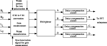
The block diagram of the delay and data preparation card (delay-DPC)
is shown in Fig. 25.3. Each basic unit of the delay-DPC
takes the four outputs of ADCs corresponding to (see Fig 25.1)
the signals ![]() and
and ![]() from a given antenna. These 6 bit
quantized signals are rounded off to 4 bits and then sent to a
multiplexer. The multiplexer has various modes; for example any one of
the four inputs of the multiplexer can be mapped to all four of its
outputs (
from a given antenna. These 6 bit
quantized signals are rounded off to 4 bits and then sent to a
multiplexer. The multiplexer has various modes; for example any one of
the four inputs of the multiplexer can be mapped to all four of its
outputs (![]() in Fig. 25.3). Other mappings include
(a)
in Fig. 25.3). Other mappings include
(a) ![]() ,
, ![]() ,
, ![]() ,
, ![]() , and (b)
, and (b) ![]() ,
,
![]() ,
, ![]() ,
, ![]() , which are used for polarization
observations with the correlator. The multiplexer outputs are
passed through a memory based integral delay compensation circuit
(see Chapter 9). The delay compensated outputs are
then fed to the FFT subsystem.
, which are used for polarization
observations with the correlator. The multiplexer outputs are
passed through a memory based integral delay compensation circuit
(see Chapter 9). The delay compensated outputs are
then fed to the FFT subsystem.
The rate at which data is written to the memory in the dly-DPC
card is tunable. In particular it can be any one of ![]() MHz,
where
MHz,
where
![]() . This rate is chosen to be the Nyquist rate for the
input signal bandwidth, i.e. for bandwidths smaller than 16 MHz, the
rate is less than 32 MHz. However, the data is always read out at
a constant rate of 32 MHz25.3. To maintain the data throughput, data from
the memory hence has to be read out in an `overlapping' fashion. This
way of reading the data provides the facility to perform `overlapping'
FFTs (and hence an improvement in the signal to noise ratio) when the
input bandwidth is less than 16 MHz.
. This rate is chosen to be the Nyquist rate for the
input signal bandwidth, i.e. for bandwidths smaller than 16 MHz, the
rate is less than 32 MHz. However, the data is always read out at
a constant rate of 32 MHz25.3. To maintain the data throughput, data from
the memory hence has to be read out in an `overlapping' fashion. This
way of reading the data provides the facility to perform `overlapping'
FFTs (and hence an improvement in the signal to noise ratio) when the
input bandwidth is less than 16 MHz.
The two other functions of the delay-DPC system are (a) gain measurement (b) Walsh demodulation.