GMRT INTRODUCTION
NCRA has set up a unique facility for radio astronomical research using the metre wavelengths range of the radio spectrum, known as the Giant Metrewave Radio Telescope (GMRT). It is located at a site about 80 km north of Pune. GMRT consists of 30 fully steerable gigantic parabolic dishes of 45m diameter each spread over distances of upto 25 km. GMRT is one of the most challenging experimental programmes in basic sciences undertaken by Indian scientists and engineers.
Apart from the novel low-cost design of the parabolic dishes, the instrument has state-of-the-art electronics systems developed indigenously and consisting of the following main sub units.
1. Antenna feeds at six different frequency bands between 50 MHz and 1500 MHz, having good polarization characteristics as well as simultaneous multiband operation.
2.Low-noise amplifiers, local oscillator synthesizers, mixers, IF amplifiers.
3.Optical fibres linking the entire array with the CEB. These are used both for the telemetry signals and local oscillator phase reference communication between the CEB and each antenna base.
4.Digital Backend (Correlator System).
Digital Backend:
The initial design and development of correlator system started in the year of 1991. It was 2 antenne, then 4, 8, 16 and 32 antennae correlator. The 30-station single side-band, dual polarization, ~230,000 channel FX correlator has been installed in the CEB in August 1998. This correlator is designed to generate 128 spectral channels spread over a maximum bandwidth of 16 MHz for each of the polarizations. Fringe stopping and fractional sample time correction is done in the hardware. The design of the correlator for the second side-band started. Full pledged correlator of 30 antennae, both polarizations & 32MHz bandwidth started working since June 2002. This hardware correlator was mainly ASIC based FFT and MAC boards. A digital 2,30,000-channel FX-type correlator providing upto 128 spectral channels and covering a maximum bandwidth of 32 MHz. This backend also had the pulsar backend of Incorreherant array (IA) and Phased Array (PA).
In the year 2009, GMRT Software Backend (GSB) integrated and released for internal observations, which was under design and development since 2003. Once this GSB system got stabilized, in the year 2010 the ASIC based correlator and pulsar systems dismantled forever. GSB system is the main backend being used for observations as on today.
In the year 2006, started design and development of FPGA (ROACH boards) based correlator. Initially single board 2 antennae pocket correlator, then 4, 8 & 16 antennae packetized (multi modular) correlator built. The signle board design modified to use for 15 meter project at NCRA campus in the year 2014.
Apart from the design and development of these backends needed to upgrade the GMRT project capabilities, the group also done the study and development of many other projects like RFI mitigation algorith, temperature study and monitoring etc..
32MHz(GSB) INTRODUCTION
GMRT Software Backend (GSB) has been designed, developed and released for observations in the year 2010. Once this GSB got stabilized, the ASIC based correlator, which was in use for more than 8 years was dismantled. The key details about the GSB are as follows:
Radio Astronomy Signal Processing Blocks:
1. Sampling of Analog data
2. Delay compensation – Integer delay
3. Fringe Rotation
4. FFT
5. Cross-correlation -- MAC
6. Recording of integrated visibility data
GSB:
Correlator :
Input data rate : 1.9 Gsamples/s
Output visibilities at 128 ms rate
256 spectral channels across
32 MHz BW for total intensity mode;
full polar mode at half the BW
Supports sub-array mode of GMRT
with different sources / frequencies
for each sub-array
Uses mostly ASICs + some FPGAs
Pulsar Receiver:
1. Delay and phase corrected data from the FFT outputs is given to the GMRT Array Combiner (GAC)
2. The GAC allows any user selected set of antenna signals to be added to get the array output
3. Supports 2 modes (simultaneous operation)
incoherent array -- power sum
phased array -- voltage sum
4. Can do simultaneous multi-frequency observations with a single pulsar receiver -- trade-off BW for different sub-arrays
32MHz(GSB) IMAGES
GSB to GWB channel mapping
Net Sign conventions in LTA file (-/+1)
NET_SIGN = { USB(R), USB(L), LSB(R), LSB(L) }

e.g. NET_SIGN = { 1, 1,-1,-1}

USB => upper side band
LSB => lower side band (not in use)

R   => 130 / right polarisation  (pol1)
L   => 175 / left  polarisation  (pol2)

 1  => frequency increases with channel number.
-1  => frequency decreases with channel number.

GSB => gmrt software  correlator/backend, 16.6/33.3 MHz (max).
GWB => gmrt wide band correlator/backend, 200/400   MHz (max).

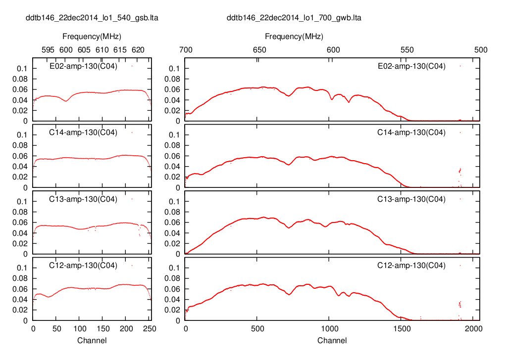
Band Plot
Left plot GSB (591 to 624.33 = 33.33 MHz)               Right plot GWB (700 to 500 = 200 MHz)
NET_SIGN = { 1, 1,-1,-1}                                NET_SIGN = {-1,-1, 1, 1}

BROADBAND(GWB) INTRODUCTION
MRT is upgrading to uGMRT and the back-end systems are undergoing major changes to achieve the upgrade system specifications like increased bandwidth of 400MHz, direct processing of RF signals, increased dynamic range, improved channel resolution. The digital backend part of this upgrade was named GWB(GMRT WIDEBAND
BACKEND). As part of this upgrade, a version of GWB(GWB-II) has been built and released for users. This is a 4-antenna dual polarization or 8-antenna single polarization correlator developed on CPU-GPUs and FPGA boards.
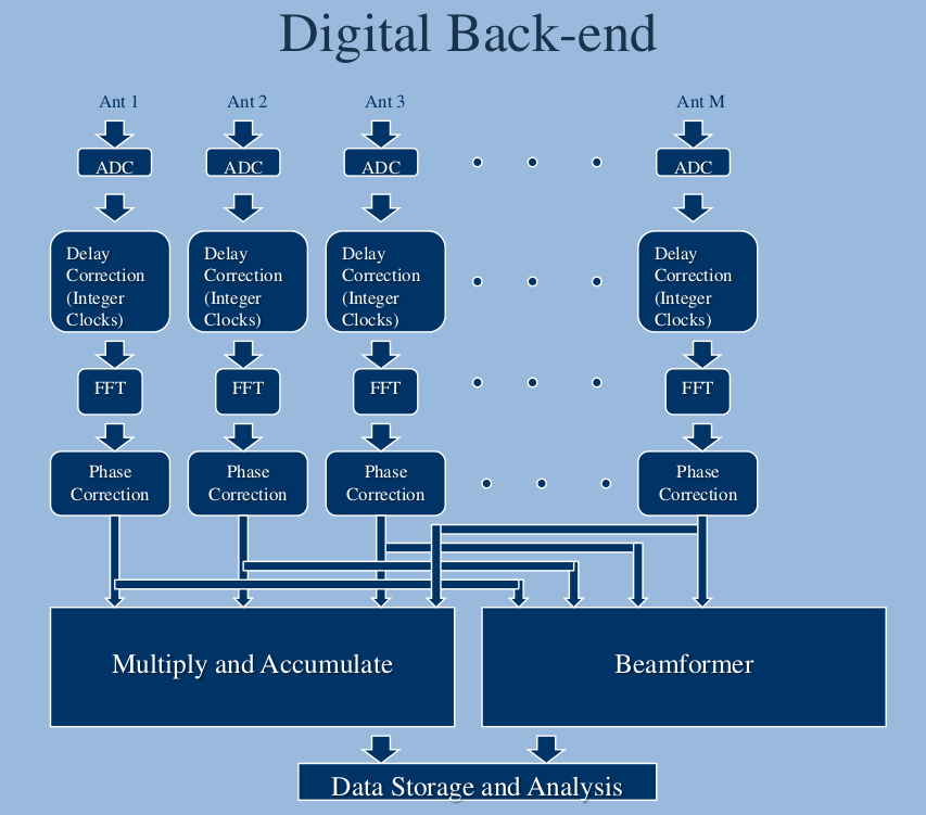 Fig : Digital Back-end
The design is a hybrid one using FPGAs and CPU-GPUs for various processes in the digital back-end chain. FPGAs connected with ADCs perform the digitisation and packetising the data while CPU-GPUs acquire the data, perform correlation and record the visibilities onto a disk for post-processing and analysis.
BROADBAND(GWB) IMAGES
GSB to GWB channel mapping
Net Sign conventions in LTA file (-/+1)
NET_SIGN = { USB(R), USB(L), LSB(R), LSB(L) }

e.g. NET_SIGN = { 1, 1,-1,-1}

USB => upper side band
LSB => lower side band (not in use)

R   => 130 / right polarisation  (pol1)
L   => 175 / left  polarisation  (pol2)

 1  => frequency increases with channel number.
-1  => frequency decreases with channel number.

GSB => gmrt software  correlator/backend, 16.6/33.3 MHz (max).
GWB => gmrt wide band correlator/backend, 200/400   MHz (max).

Band Plot
Left plot GSB (591 to 624.33 = 33.33 MHz)               Right plot GWB (700 to 500 = 200 MHz)
NET_SIGN = { 1, 1,-1,-1}                                NET_SIGN = {-1,-1, 1, 1}

Single Board (Pocket) Correlator INTRODUCTION
The POcket COrrelator (POCO) is , single FPGA based correlator.This design accepts signals from 2 antenna's single polarization through iADC.The ADC samples at 400 Mhz clock giving 8bits of digitized data per pol. The digitized data goes through Delay correction followed by 1024 point FFT , FSTC , Fringe correction is done. Then data is integreated for 1 sync ( 1 sync = 1.34 seconds). The integreated data goes to control PC through 100Mbps link.
Single Board (Pocket) Correlator Documents
| Released Date |
Version |
Description |
Remarks |
Single Board (Pocket) Correlator Images
Modular Board (Packetized) Correlator INTRODUCTION
The aim of the project is to implement a correlator for large number of antennas. This involves splitting the design into F-engines & X-engines and sending the data from Fengine to Xengine in the form of packets via 10Gbe link and hence is called as the Packetized Correlator. The design was implemented in various phases.
Phase1: The F-engine was modified to send the data in packets by using blocks such as Corner Turner and Packetiser. This requires the modification in X-engine compared to the previous correlators on one FPGA chip (called pocket correlators). The MAC (lta block) was designed using BRAMs. The other blocks like the packetiser, mux_adc_level and XAUI_pack used in the design were developed by the KAT group from South Africa.
Phase2: 10Gbe link is used to send the data from F-engine to X-engine. This was the most challenging job faced during this period since it was not possible to simulate the 10Gbe block. Snap blocks were place in the design for debugging purpose. This helped in understanding the format of the packets on the receiving side. The design was successfully tested by sending the data of F-engine via 10Gbe to X-engine.
Phase3: The next step was to use the master counter of the received packets for synchronization with the packets from the direct link. This scheme of checking with the master counter will ensure that even if the packet is dropped by the 10Gbe only appropriate packets with same master counter will be considered as the useful data.
Packetised Beamformer IA (4-antennae):
four ROACH boards each with one iADC card is used. Each iADC card has a clock, sync and two inputs for signal . While the clock & Sync input is a must for all iADC cards. Each GPU PC (a total of 4 GPU PCs) is equipped with two 10 GbE cards apart from the GPU card. One 10 GbE card is directly connected to one of the two ROACH boards while the other 10GbE card is connected to neighbouring GPU PCs via a 10 GBE switch.
Number of F-engines : 4 and Number of X-engines : 8
After programming the ROACH with the BOF_FILE and configure parameters like the IP address and port of the destination 10gbE, the ROACH starts sampling the input signals given to the iADC card and makes UDP packets that can be sent over 10GbE. The size of packet is 8k bytes with 4k bytes of data from each iADC input signal. Gulp captures the packets along with the header.
Modular Board (Packetized) Correlator Documents
Modular Board (Packetized) Correlator Images
INTRODUCTION
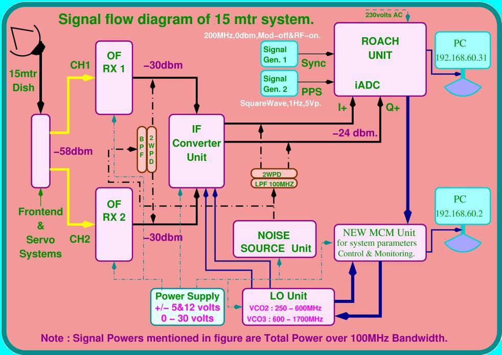
The Correlator for 15 meter is a single FPGA based (ROACH board with one iADC card) correlator. This design accepts signals from both polarization of single antenna through iADC. The ADC samples at 800 MHz clock giving 8bits of digitized data per pol. Two modes are supported by this design viz. Correlated output for real time analysis and raw ADC data for offline analysis.
Real Time mode : In real time mode 1024 point FFT is done on the digitized data. The data is intergrated for 1 sec. The final output goes to control PC through 100Mbps ethernet.
Offline mode : The digitized ADC data is acquired via 10Gbe, hence giving flexiblity for the user to do offline correlation/analysis. The data is sent in form of 8K bytes per packet. Each packet comprises of 64 bits of header followed by data from pol 1 and 2. Each 64 bit data consist of 4 samples 8 bits from both polarization.

Analog signals from the 15 meter dish base , comes to 15mtr system in the lab through optical cable. After converted back to electrical, these signals reaches the digital backend through IF system.
The digital backend has ADC with ROACH in a single unit/box. It needs clock and PPS signals with two inputs. Clock of 800MHz , 0dbm is provided using Signal generator and PPS(Pulse Per Second) from GPS unit. Two analog inputs gets converted into digital by ADC card. Through ZDOK connector digitized signals goes to ROACH unit.In the ROACH unit data goes through Delay correction , DDC , FFT and MAC.
INTRODUCTION
SKA and LFAA
The Square Kilometer Array (SKA) is a major radio telescope that is being built by an international collaboration. The first phase of the telescope will have two arrays, SKA1-mid: a mid-frequency dish array to be constructed in South Africa and SKA1-low: a low-frequency aperture array to be constructed in Western Australia.
A major design challenge for the SKA1-low telescope comes from the enormous size of the low-frequency aperture array (LFAA). The LFAA is formed out of 131,072 wideband antennas that are optimally positioned in groups of 256 to form 512 stations across a wide area of about 40 km radius.
The LFAA signal chain consists of antennas, low noise amplifiers analog receivers, RF over fibre network, and digital signal processing to form station beams. The digital processing is implemented in a tile processor module, which is duplicated to handle 131,072 antennas that operate over 50-350 MHz band. The antenas are grouped to form 512 stations and station-wide beams that are normally 20 sq. degrees in the sky.
Digital Tile Processing Module (TPM)
The digital processing will make use of the start-of-the-art ADCs and FPGAs. The channelization is performed using a polyphase filter implemented in the FPGAs. The compensation for delay/gain/weight help in pointing the beam in a particular direction. A real-time programmability of these parameters is required at desired intervals for the normal telescope operation. A programmability will also be required to select the frequency channels required for the beams, and possibly excluding the channels with gross RFI. Currently, one ADC/FPGA TPM board is used to process 16 dual polarized antennas.
The LFAA Subrack system is the basic structure required to integrate the iTPM–ADU boards within the Rack: the iTPM-ADU is the main board managing Analog to Digital conversion and pre-processing of a multi-channel source in the LFAA.
The Subrack is composed by:
• Backplane board to move all the required services, needed by iTPM-ADU, from the front-panel to the opposite side
• Management board, plugged on the Backplane, providing relevant functions as interfacing the Rack Ethernet network to the iTPM-ADUs, distributing/regenerating the synchronization signal to the iTPM-ADUs, managing/monitoring the Subrack power supply, power distribution, FANs, providing a Linux-based CPU
• Commercial power supplies
• Adapters board to interface the power supplies
• 4 commercial fans
e-GMRT
e-GMRT stands for Expanded Giant Metrewave Radio Telescope, which is having Parts such as,
1. Extended Baseline
2. Shorter Baseline
3. Focal Plane Array
Documents : Focal Plane Array
RFI INTRODUCTION
To develop RFI mitigation algorithms using statistical approaches like standard deviation, median absolute deviation and kurtosis. These calculations are ultimately given as a clipping threshold to the voltage time domain clipper module. The voltage time domain clipper carries out a time domain analysis of RFI and replaces it by a blanking data.
Implementation: The module accumulates 8bit data and the square of the data for 1024 clock cycles. The accumulator sizes for mean and mean square are 19 and 25 bits respectively. Then, it averages this data, dividing it by 1024 (shifting the data). The variance is calculated by subtracting the mean and mean square (average) and then calculating the square root of the difference. The square root calculation is done using a lookup table based approach. The variance calculated is multiplied by a factor, received as an input by this module (say n*sigma).
This value mean + (n*sigma) and mean – (n*sigma) is compared with the input data and a signal is provided to the multiplexer when the values exceed this level. Based on an input signal to this module, the data above this limit is blanked either with a noise or a fixed pattern or a null. When the reference values for sigma and mean are being calculated, there is a provision to bypass the data to the output multiplexer.
SIGNAL PROCESS BLOCK
The Signal-Processing Block comprises of four main subsystems :
1.The Analog-to-Digital-Conversion(ADC) Subsystem: Digitises the incoming analog signals.
2.The Delay Subsystem: Compensates for the geometrical and the instrumental delay in the appropriate digitised data streams.
3.The Fast Fourier Transform(FFT) Subsystem: The F part of FX. Perform frequency analysis on the sampled data to provide the spectrum.
4.The Multiply and Accumulate(MAC) Subsystem: The X part of FX. Computes the auto and cross correlation between every spectral provided by the FFT Subsystem.
HIRARCHICAL CONTROL BLOCK
The Hierarchical control is achieved by distributed elements employing embedded processors at subsystem level, all networked to form the following pyramid:
1.Embedded Control Cards: The Delay, FFT and MAC Control Cards form the embedded layer. They are the last in the control chain - the base of the control pyramid - and interact directly with the data processing block. They are situated in the subsystem subracks and provide various information to the Delay, FFT and MAC subsystems respectively.
2.The Rack Control: Handles rack level tasks such as monitoring of temperature, voltage and current. Will also be responsible for remote shutdown of the power-supplies in case of an emergency. Forms a liaison between the Master Control Card and the embedded layer.
3.The Master Control Card(MCC): Performs a variety of tasks. It is the communication link between the Correlator Control Computer and the rest of the correlator. Generates and distributes clocks, synchronisation, and initialisation signals to all control cards.
4.The Correlator Control Computer(CCC): This is the host of the Correlator Control system. This is the part of the correlator wihch is visible to the outside world. This collects information about array configuration, source being tracked, etc., and dynamically evaluates the relevant parameters for various subsystems and communicates these to the MCC.
5.The Delay Subsystem:Compensates for the geometrical and the instrumental delay in the appropriate digitised data streams.
6.The Fast Fourier Transform(FFT) Subsystem: The F part of FX. Perform frequency analysis on the sampled data to provide the spectrum.
7.The Multiply and Accumulate(MAC) Subsystem: The X part of FX. Computes the auto and cross correlation between every spectral provided by the FFT Subsystem.
MASTER CONTROL CARD
The functions of the Master Control Card are:
1.Clock Distribution:32.25MHz clock to:Delay DPC,FFT Control cards,MAC Control cards,Pulsar Machine.
2.Counters:FFT Cycle = 516 clock ticks, one FFT_INIT per cycle,DLY Cycle=8k FFT cycles (128 ms approx); one DLY_LOAD per cycle.
3.Master Reset:Power On-Reset pulse.
4.MASTER_INIT:Triggered by online computer; required in every scan; Distributed to; FFT Control Cards, MAC Control Cards, Pulsar Machine.
5.FFT_INIT:One pulse every FFT cycle, during the dead-time, delayed by different amounts for DPC, FFT Control, MAC Control cards and the Pulsar Machine.
6.DLY_LOAD:Once every 8k FFT cycles;Distributed to : FFT Control cards, DPC, Pulsar and Data Acquisition System.
INTRODUCTION
The Sampler subsystem is the front-end of the correlator system. Its main task is to convert the analog signals coming from the various antennae to digital format which can be further processed. Analog signals are continuous in time and amplitude, existing at every instant of time with any possible intermediate amplitude values. DSPs mathematically process signal represented as a series of numbers that are discrete in time and amplitude. Analog to Digital Conversion (ADC) consists of sampling, hold, quantize and code. Sometimes these four functions are integrated into one device(ADC card).
1.Sampling:
Sampling converts a signal that is continuous in time to one that is discrete in time. Sampling is done in accordance with the Nyquist Theorem that states that if sampling is performed at a rate exceeding the Nyquist rate or two times the bandwidth of the signal, no signal information is lost. The number of samples taken per second is called the sampling rate or sampling frequency.
2.Hold and Quantize:
After sampling the signal is discrete in time but it is still continuous in amplitude. The signal is made discrete in amplitude as well by quantizing or representing each signal as a number with finite resolution. A hold function is used to maintain the sampled value constant during the time it takes to quantize the signal. Flash converters are used for this task. Flash converters use a bank of comparators and voltage references, one for each quantization level. Unlike Nyquist sampling, which loses no information, quantizing produces an error called quantizing error. The difference between the exact value and the quantized value is the quantizing error.
3.Coding:
Coding is the representation of the quantized value in a particular numerical format usually a form of binary. The various codes used for bipolar signals differ in their representation of the sign and the transition from positive to negative values.
Read More
INTRODUCTION
The maximum delay from the transmission lines from the antenna base to the CEB is of 2.048 mS (in units of 32 ns). Dynamic update in 2 sec. The Delay DPC unit of the Correlator performs the Noise switching & Walsh demodulation of the signal from the ADC Subsection. RFI mitigation in time domain is also performed. Conversion of unsigned 6 bits from ADC to 4 bits sign magnitude form is done in the Delay DPC system. Dual clock support is present to take care of extra overhead cycles in the FFT. Narrow bandwidth support for spectral line mode of observation is provided using the decimation technique ( de-sampling ) on the sampled data. Bandwidths supported ranges from 125 KHz to 16 MHz of analog Baseband signal. Channel multiplexing at the output ( as needed for the full polar mode ) is also performed. The hardware has been implemented using two Altera FPGA devices per antenna ( all 4 channels ) on one board, and PLDs for bus arbitration logics.
Read More
INTRODUCTION
Complex numbers to be multiplied and accumulated in the MAC come from outputs of the FFT cards. Two FFT cards are required to process signals from one antenna. In Indian Polar mode as well as NonPolar mode, FFTs in one side band system outputs signals from Upper Side Band and FFTs in other sideband system output signals from Lower Side Band ( total BW therefore is 32MHz ), whereas in Full polar mode all FFT cards outputs signals from same sideband ( USB or LSB total BW therefore is 16Mhz ). Each FFT card has two pipelines to process Right and Left circular polarization independently. FFT card performs N ( 512 ) point FFT on the incoming data and gives N/2 ( 256 ) channels as output. The output from two pipelines is multiplexed to maintain the 32Ms/sec data rate which is the required data rate for the MAC. Thus output from the FFT card is always in time multiplexed fashion ( R & L polarization ) but depends on the mode selected at the DPC subsystem. FFT output is in 12 bit ( 4 bits real, 4 bits imaginary and 4 bits common exponent ) format since FX ASIC in MAC mode accepts input in this format.
FFT backpanel receives output from 10 FFT cards in each rack and output from two adjacent FFT cards is combined into one using a patch PCB. This patch PCB takes 12 bit TTL output from two adjacent FFT cards via two EURO connectors and gives output on one 50 pin FRC connector with ground connection on alternate pins. This combined FFT output from two FFT cards is given to Translate system using 50 core flat ribbon cable.
Translate Subsystem converts TTL single ended output from each FFT to ECL differential form and also generates four copies ( including the one for Pulsar Machine ) of it. Therefore each Translate backpanel has three copies of 10 FFT outputs in ECL differential form.
A patch PCB used at translate backpanel acts as a adapter which takes input from translate backpanel and gives the output on single 50 pin SMT connector.Each TRANSLATE CARDessentially makes three copies of two FFT outputs. Therefore each 50 pin SMT connector at translate backpanel carries output of two adjacent FFT cards in ECL differential form.
READ MORE
INTRODUCTION
MAC sub-system Multiplies and Accumulates the signals from each pair of 30 antennas. It provides a 30x30 matrix for each of 2 sidebands & 2 polarisations, with 256 spectral channels per sideband. Visibilities are output at the rate of once every 128 ms. Number of spectral channels is :
a.128 in 32 MHz BW, Indian Polar,
b.128 in 16 MHz BW, Full Polar,
c.256 in 16 MHz BW, Non-polar.
The most integral part of the MAC Subsystem is the MAC card. The MAC card has an ASIC chip which is its fundamental element. Each ASIC takes input from 2 FFT cards, 12 bits each. The inputs go to registers and they get multiplied and then accumulated for the N number of FFT cycles. The accumulated data of one cycle is stored in the first bank of the ASIC RAM, which is 256 * 36 ( # of spectral channels * Bits in output 15,15,6 ). In the next cycle, MAC operation uses the second bank of the ASIC RAM. During the four dead cycles, the Data goes to the acquisition machine through back plane and DAS card.
READ MORE
G.M.R.T CLOCK
The GMRT clock operates at 32MHz. The FFT chips used for the GMRT correlator require 4 extra clock cycles for performing a 512 point FFT ( Fast Fourier Tramsform ). The GMRT samplers operate at 32MHz. Thus to maintain the data throughput, the FFT ( and MAC subsystem ) subsystem can be operated at 32.25MHz ( = 32MHz x 516/512 ). In this scheme, the delay-DPC subsystem takes the data from the sampler at 32MHz and sends to the FFT subsystem at 32.25MHz. For synchronising the data flow at the two clock rates in the delay-DPC a synchronising signal is required. An elctronic circuitry has been built using two DDSs ( Direct Digital Synthesiser ) for the generation of 32MHz and 32.25MHz clocks and the required synchronisation signal.
READ MORE
ASIC Correlator SOPs
| Released Date |
Version |
Description |
Remark |
|
INTRODUCTION
This instrument namely the G.M.R.T. Array Combiner ( GAC ) is designed to facilitate the single beam made observations for G.M.R.T. Some of the astronomical observations planned with G.M.R.T. can be effectively carried out using these single beam modes. Two of the possible single beam modes are considered here. One of which is the Incoherent Array ( IA ) output and the other one is the Phased Array ( PA ) output. The Phased Array output is formed by coherently combining outputs from the array elements. This is useful for observations of small sky area that require a very high sensitivity. It is very useful for the survey kind of observations. Both are available simultaneously to facilitate more than one kind of observations possible at the same time. It is possible to apply gain correction in GAC to equalise the gain difference along the pass band. The GAC hardware is realised using the PROM based pipe-lined combiner network.
INTRODUCTION
This instrument namely the G.M.R.T. Array Combiner ( GAC ) is designed to facilitate the single beam made observations for G.M.R.T. Some of the astronomical observations planned with G.M.R.T. can be effectively carried out using these single beam modes. Two of the possible single beam modes are considered here. One of which is the Incoherent Array ( IA ) output and the other one is the Phased Array ( PA ) output. The Phased Array output is formed by coherently combining outputs from the array elements. This is useful for observations of small sky area that require a very high sensitivity. It is very useful for the survey kind of observations. Both are available simultaneously to facilitate more than one kind of observations possible at
the same time. It is possible to apply gain correction in GAC to equalise the gain difference along the pass band. The GAC hardware is realised using the PROM based pipe-lined combiner network.
READ MORE
POLARIMETER FOR G.M.R.T.
During the past thirty years of Pulsar research, several sensitive observational experiments have been conducted to discover pulsars and study their properties in detail. The current sensitive limit is about a milli-Jansky for Pulsar searches and much better for Pulsar studies. To reach this sensivity, the surveys use low frequency telescopes with large apertures, large R.F. bandwidth and the observed time sequence is folded with the pulsar period for several thousands of periods. It is also required to remove the effects of dispersion, Faraday rotation and Doppler acceleration and integrate the power in time and frequency for maximising the sensitivity. The data rate of the digitized samples at the output of these receivers runs over a hundred Mbytes per second, also making it extremely difficult to store the raw data of large bandwidths. The offline-processing jobs demand high through-put of the order of several giga-operations-per second. In practice, a hybrid solution is sought using dedicated, real-time processing instruments to perform specific real-time processing tasks so as to reduce the data volume and post processing rate. So far, such instruments have been limited in their flexibility to handle different types of pulsar observations and cater to small bandwidths) typically a few MHz). A Polarimeter has been developed for the G.M.R.T. at the Raman Research Institute, Bangalore, India. The Polarimeter is designed primarily for use with the G.M.R.T. radio telescope and perform the above mentioned operations over dual, orthogonal-polarization data samples of 512 frequency channels covering a maximum bandwidth of 32MHz. The digital design exploits the advantages in using look-up tables, reprogrammable logic circuits and DSP chips to provide full programmability and a modular architecture so that the bandwidth can be scaled from 1MHz to 32MHz and interfaced to work with any other telescope. The optimizations used in the signal processing algorithm and their software implementation are also discussed.
READ MORE
INTRODUCTION
The first block of the pulsar receiver is the GMRT Array Combiner ( GAC ), built by the Raman Research Institute, Banglore. It combines the signal from a maximum of 30 antennas for both incoherent and coherent array operation. In both cases, the signals have 256 spectral channels, which are generated by the FFT units ( which are part of the FX correlator used at GMRT ). For all data output by the GAC, the sampling rate is 16 micro second.
The two back-ends allow the raw data stream from the GAC to be integrated in time / frequency to achieve a net data rate at which the signals can be recorded using PC based data acquisition systems. In addition, the PA bin computes the basic self and cross terms between the voltage signals of the two polarizations, from which the full Stokes parameters can be constructed. The highest time resolution achievable is 128 microsec for the IA mode and 512 microsec for the full Stokes PA mode. These back-ends are available only for one sideband ( 16 MHz ) BW and are connected to the upper sideband ( USB ).
Learn about the Pulsar modes of GMRT.
READ MORE
Pulser Backend SOPs
| Released Date |
Version |
Description |
Remark |
|
WALSH Mod/Demod.
In GMRT there are 30 antennas with dual polarization channels from each antenna providing 60 RF signals.
Signals from one antenna could leak into another antenna at various points along the signal flow chain.
This is normally referred to as cross-talk. This would cause a spurious correlation between the baseband signals from these
two antennas.
The effect of leakage can be minimized by switching the phase of the RF signal of each antenna by a pattern
that is ortho-normal to the pattern used for all other antennas. At the correlator the exact reverse phase switching is
done for each anteena so that the original phase is recovered just before the cross correlation is done such a scheme would
greatly reduce the cross talk at all points between the RF amplifier and base band.
Presentations : 32MHz(GSB)
| Date |
Presenter |
Description |
Remark |
Presentations : BROADBAND(GWB)
| Date |
Presenter |
Description |
Remark |
Presentations : Other Backends
Presentations : Mini Projects
GMRT & DIGITAL BACKEND Images

 Fig : Digital Back-end